Copackaged Optics - Shrinking the Distance Between Copper and Light
As AI clusters grow, light is aggressively eating the territory copper used to own. Copper wins on price but can it keep up with the ever increasing bandwidth demand?

GPUs in a datacenter communicate from one corner of the warehouse sized datacenter to another corner which may be 50 meters away. Copper physically cannot do this at the speeds AI demands. The current Ethernet switches used have speeds of 800 Gigabits, with 1.6 Terabits per second switches coming up.
Let’s try to understand why Co-Packaged Optics is the answer to copper interconnects hitting their physical limit.
Scale In vs Scale Up vs Scale Out vs Scale Across
GPUs are first integrated into a server to form a GPU compute node. Multiple nodes are then interconnected through a high-speed network to build a multi-node GPU cluster. Within a single server, multiple GPUs are also linked through board-level high-speed interconnects to form an internal single-node GPU cluster.
This article is the holy grail of how communication happens in a GPU rack.

Scale in refers to the integration of computing resources within the smallest possible domain specifically at the silicon, chip, and package level.
Scaling up typically happens within a single GPU rack. Copper is the most cost-effective way to handle high-bandwidth internal connections (like 100G or 400G). However, copper has a physical wall. As you try to push more data over longer copper cables, signal degradation and electromagnetic interference become massive hurdles. It means adding more GPUs inside one server and connecting them through a high-bandwidth interconnect.
GPUs communicate with each other using the NVLink. NVSwitch acts as a switching layer, with each link connecting a GPU to the NVSwitch. Communication travels only through PCB copper traces.
As you Scale Out, the infrastructure spreads across dozens of racks and entire server rows. At this stage, copper becomes too heavy, too thick, and too limited in range. Optics allow for much thinner cabling, which is essential for airflow and cooling in a scaled-out environment.
Multimode fiber (MMF) has a wider core (~50 µm), which causes light to bounce around inside the fiber, taking multiple paths. This leads to higher signal dispersion, meaning the signal degrades more quickly. MMF uses lower-cost VCSEL (Vertical-Cavity Surface-Emitting Lasers), making it ideal for short-range data center interconnects. The trade-off is the cost of the transceivers (the modules that convert electricity to light).
Each AI server typically carries high-speed NICs (Network Interface Card) dedicated to compute traffic. These NICs connect to the ToR (top-of-rack) switch through optical links. Scale Out relies on standard InfiniBand or Ethernet technologies. RDMA is the dominant communication method, using either InfiniBand or RoCEv2 over Ethernet.
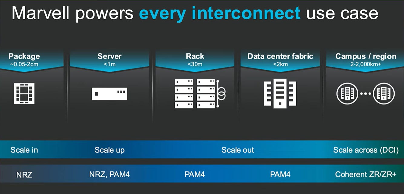
When you move to Scaling Across, you are dealing with distances that span kilometers between datacenters or thousands of miles between regions. Unlike the bouncing light paths in multimode fiber, Single-mode fiber uses a focused laser that travels in a straight line, allowing it to maintain signal integrity over vast distances without the need for frequent amplification. Single-mode fiber (SMF) has a narrow core (~8-9 µm), allowing light to travel in a straight, single path, minimizing dispersion and enabling long-distance transmissions (500m – 10km+). It leverages laser-based sources like Electro-Absorption Modulated Lasers (EMLs) or Distributed Feedback (DFB) lasers.
While the laser equipment is the most expensive of all, it provides the nearly infinite bandwidth required to sync global databases. These data centers are interconnected through high-speed optical links and DCI/WAN/metro routers and switches. The network may include high-bandwidth channels such as 800G or 1.6T to support large volumes of model traffic and data movement.
Copper for scale up. Optics for scale out.
Just to recap - Scale-out is the network between a GPU rack and another GPU rack. Scale-up is network connectivity inside the GPU rack.
Optical modules have more potential points of failure. Lasers degrade over time, connectors are sensitive to dust and misalignment, and the components are vulnerable to both heat and electrostatic discharge.
Again, the faster you transmit data (shorter the pulses) and the longer the cable, the worse the resulting signal at the other end. Basically, you have to choose between long cables or fast data transmission, and there’s a ceiling on both.
The extra thick diameter of high frequency cables doesn’t change the skin depth, but it does increase the surface area available for current to flow through, decreasing resistance a bit. At high frequency, the impedance causes attenuation.
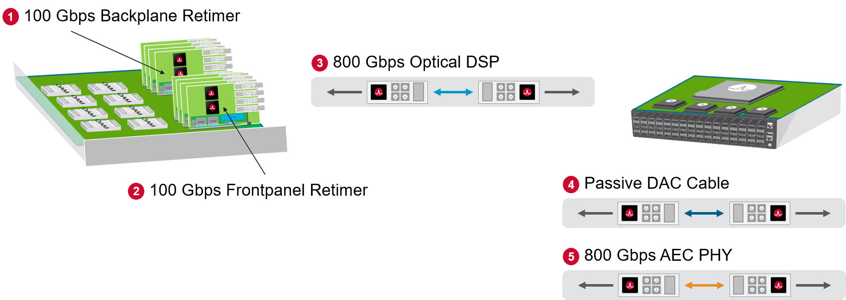
A single high-performance NVIDIA GB200 NVL72 rack uses over 5,000 copper cables. Copper cabling is the lowest cost, lowest latency, and lowest power way to interconnect high-speed system racks within the 3-meter maximum length.
5,184 passive‑copper NVLink cables to connect GPUs inside the rack. These DACs are perfect for scale‑up, where everything stays inside a single rack and latency must be as close to zero as possible.
In scale-out, the distances are longer, the topology becomes switch‑based, and the signaling is Ethernet or InfiniBand rather than NVLink. Copper alone cannot maintain 800G/1.6T signal integrity over these distances, so this layer uses ACC or AEC cables. ACC extends copper reach with analog equalization, while AEC adds a full digital retimer to guarantee signal quality.
Direct Attach Copper cables (DACs) “directly attach” the electrical subsystems together, hence the name . And if you were to extend over several racks, LACC(Linear Active Copper Cables) are used which come with an additional IC in each end to boost the signal power and noise reduction. DAC is Passive Electrical Cable and LACC are known as AEC (Active Electrical Cable) because there are chips actively doing the signal processing.

Why Co-packaged optics?
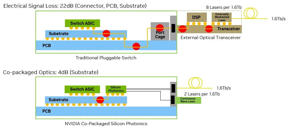
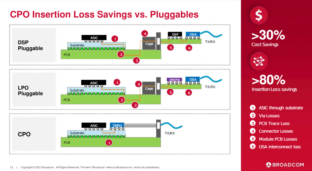
The reason we are moving to Co-Packaged Optics (CPO) is to get rid of the need for so many Retimers and DSPs. It converts the signal to light immediately and it doesn’t need to be cleaned up. As bandwidth needs rise, the traditional way of transmitting electrical signals to pluggable optical transceivers at the edge of a server is becoming too power‑hungry and inefficient. The long electrical traces, signal degradation, and heavy use of SerDes circuitry all add significant power, heat, and cost. This has driven the industry to explore new approaches from Linear Pluggable Optics (LPO) to Co‑Packaged Optics (CPO) to shorten electrical paths and move optical conversion closer to the compute silicon.
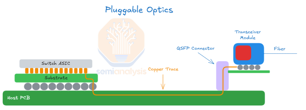
Today, almost all electrical‑to‑optical conversion happens inside pluggable optical transceivers. Pluggable optics have the laser source in a small form factor pluggable (SFP) device that has a full optical transceiver in a compact connector that plugs into the front of the rack.

We shall talk about how the optical interconnect is shaping up for future networking -
Gen 1 - DSP Pluggable transceivers
Data starts at the GPU/Switch chip (ASIC), travels across 10–20 cm of copper traces on the circuit board, and then enters the transceiver plugged into a cage at the front or back of a server. At high speeds (800G+), the electrical signal weakens so fast that it requires DSPs (Digital Signal Processors) or Retimers to push the data across the board. This creates a thermal wall where the system gets too hot to function efficiently.
The transceiver takes the electrical signal, cleans it up using an optical DSP, and then sends it to optical components that convert it into light. That light travels over fiber to the far end, where another transceiver converts it back into electrical form for the destination chip.
DSPs use math to fix signal distortion. Marvell’s Alaska A and Nova lines are the industry standards for 800G and 1.6T links. Retimers catch a fading signal and re-transmit a fresh, clean copy of it. Marvell’s Alaska P family is specifically built for this. Without these retimers, its physically tough to fit 8 or more GPUs into a single server tray because the wires would be too long for the signal to survive. You need a Retimer every few inches to keep the signal alive as it travels over copper traces.
DSP‑based transceivers include an optical engine with drivers and modulators for sending signals, plus a TIA (transimpedance amplifier) and photodetector for receiving signals. The DSP chip also called Retimer handles retiming, error correction, and compensation for losses over the long electrical path from the host chip to the front‑panel transceiver. With PAM4 modulation, the DSP converts binary data into four voltage levels to increase data rate. The jump from 100G to 400G forced data centres to adopt PAM4 because it allows for two bits per symbol. This effectively doubles the data rate without needing to double the bandwidth.
Difference between DSP, Retimer and SerDes
SerDes (Serializer/Deserializer) is the underlying technology that transforms parallel data to serial (and vice versa) for transmission. It includes Clock Data Recovery (CDR) to handle signal timing. It takes wide ,slow parallel data from inside a chip (like 32 bits at 1 GHz) and squashes it into a single, ultra-fast serial stream (like 32 Gbps).
In modern high-speed systems like PCIe 5.0 or 6.0, a Retimer actually contains SerDes blocks inside it. It is a universal technology used in both copper and fiber systems. At high speeds (above 500 MHz), traditional parallel copper buses fail due to clock skew, where bits sent at the same time arrive at different times and crosstalk between adjacent wires. SerDes solves this. A SerDes is a circuit that converts data between parallel and serial formats. Squashes multiple slow lanes into one fast lane.
This isn’t unique to data center chips; even consumer SoCs like Apple’s A‑series or Qualcomm’s Snapdragon rely on high‑speed SerDes to move data from cameras, displays, and other high‑bandwidth components.
DSP (Digital Signal Processor) - Modern SerDes (especially PAM4) use DSP modules to perform advanced equalization, filtering, and error correction to improve signal quality. The signal is so distorted that simple electrical re-timing isn’t enough. The DSP performs heavy math to save the data.
a. ADC Sampling: It converts the incoming analog electrical wave into a series of numbers using an Analog-to-Digital Converter (ADC).
b. Advanced Equalization: It uses algorithms (like FFE or DFE) to calculate what the signal should have looked like, effectively cancelling out noise, reflections, and interference.
c. Error Correction: It manages Forward Error Correction (FEC), which adds extra "parity" bits to the data so the DSP can fix any bits that were flipped by noise during transmission
Retimer is device that sits between two points to clean up and re-drive a signal. It uses SerDes technology (with CDR and often DSP) to completely regenerate the signal (Rx to digital, then back to analog Tx). It utilizes high-speed SerDes technology often incorporating DSP algorithms to regenerate signals. A retimer is a standalone integrated circuit (IC). It receives a messy, attenuated signal that has travelled too far and uses its own internal Clock and Data Recovery (CDR) circuit to figure out the original 1s and 0s.
The Receiver (RX) side of a retimer uses a Deserializer to turn the incoming distorted high-speed signal back into a clean digital format. The Transmitter (TX) side then uses a Serializer to send that clean data out again as a brand-new high-speed stream
SerDes scaling is approaching a plateau.
Doubling bandwidth per copper lane by developing faster SerDes is challenging. CPO can deliver the better scaling of bandwidth.
Today’s copper-based scale-up solutions, such as NVLink, provide tremendous bandwidth of 7.2 Tbit/s per GPU but copper-based links are limited in range to two meters at most, meaning the scale-up domain world size is limited to one or two racks at most. It is also increasingly difficult to scale bandwidth over copper. Tomahawk 6 (TH6), code-named Davisson, is the fastest CPO-based network switch available in the market today at 102.4 Tbps aggregate switch bandwidth, and is primarily aimed at scale-out applications.
Higher speeds can only be sustained over very short distances without additional signal recovery components which in turn increase complexity, cost, latency, and power consumption. It has been difficult to get to 224G SerDes. Achieving true 448G uni-directional SerDes will require further development. We may need to move to higher orders of modulation such as PAM6 or PAM8 instead of the PAM4 modulation which has been prevalent since the 56G SerDes era.
In the NVLink protocol, bandwidth in NVLink 5.0 has increased more than 11x compared to NVLink 1.0. However, this growth has not come from a significant increase in lane count, which has only risen slightly from 32 lanes in NVLink 1.0 to 36 lanes in NVLink 5.0. The key driver of scaling has been a 10x increase in SerDes lane speed, from 20G to 200G. In NVLink 6.0, however, Nvidia is expected to stay on 200G SerDes, meaning it will have to deliver a doubling in lane count. It delivers on this cleverly by using bi-directional SerDes to effectively double the number of lanes while using the same number of physical copper wires. Beyond this, scaling either SerDes speed and overcoming limited shoreline availability to fit more lanes lane count will become increasingly difficult and total escape bandwidth will be stuck.
Gen 2 - LPO (Linear Pluggable optics)
DSP is one of the most expensive and power‑hungry parts of a transceiver. We can move the DSP out of the module today because modern host-side SerDes (the chips in the switch/NIC) have become powerful enough to handle the signal equalization that the module used to do. LPO was introduced to remove the DSP and rely on the high-performance switch ASIC to directly drive the optical components.
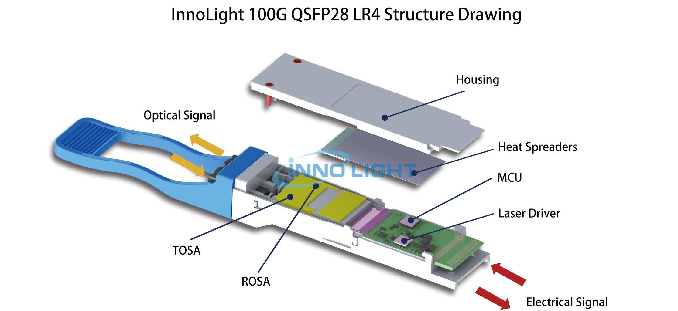
SFP (Single Form Pluggable) module consists of a transmitter optical sub-assembly (TOSA) consisting of a driver IC that drives a laser diode. The receiver optical sub-assembly (ROSA) has a diode photodetector and a trans-impedance amplifier (TIA) that amplifies the detected optical signals. If there are any optical failures, this whole connector and optical fiber assembly can be easily swapped out.
Gen 3 - External Laser Source or CPO
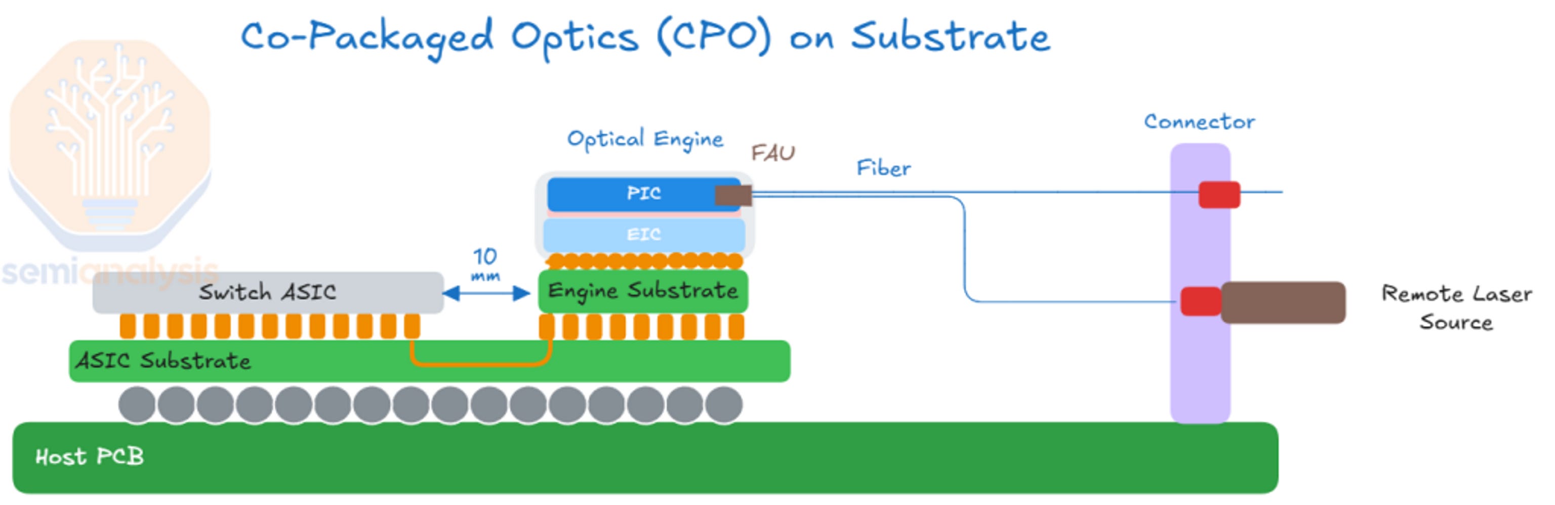
Co-packaged Optics takes this optical transceiver and integrates it next to the switch ASIC on the same package. We are fundamentally redesigning the transceiver by breaking it apart and moving its components closer to the brain of the switch.This shortens the electrical path from tens of centimeters to just a few millimeters. The result is lower power, higher bandwidth density, and lower latency
The electrical-optical conversion that was happening in the connector, now happens in a silicon photonics (SiPho) chip right next to the silicon ASIC.
On-chip laser approach combines the laser and the modulator in the same piece of silicon, usually by bonding specialized III‑V semiconductor materials like indium phosphide onto the silicon photonics platform. On‑chip lasers seem elegant because everything lives on a single chip, light loss is minimal, and the overall system is simplified. But they come with practical challenges. Heat, reliability, manufacturability, and yield issues become much harder to manage when a delicate laser sits right next to a power‑hungry GPU or switch ASIC. As a result, most companies have moved away from this approach for large‑scale systems.
External Laser Source sits in a separate module located safely away from the hot silicon. It sends continuous light into the optical engine through a tiny fiber. Because the GPU or switch ASIC generates significant heat, keeping the laser off the main package is essential. When lasers heat up, their energy bandgap shrinks, causing the emitted light to shift toward longer wavelengths. That shift may seem small, but for high‑speed optical links it can be enough to break the communication channel. By placing the laser outside the package, it stays cool, stable, and easy to replace if it ever fails. This is why the industry has broadly aligned around ELS as the practical and scalable path forward.
By relocating laser sources away from the switch ASIC to front-panel modules, CPO systems can maintain lasers at controlled temperatures while preserving hot-swap serviceability.
Pluggable optics have major advantages - they are interchangeable and easy to replace. Technicians can simply unplug and swap them. With CPO, however, if an optical engine fails, the entire switch may become unusable. The laser is the part most likely to fail, which is why thy use pluggable ELS (external laser sources). Still, concern remains about failures in non‑replaceable CPO parts.
In a paper presented at ECOC 2025, Meta showed that a standard 800G pluggable transceiver (2×FR4) uses around 15 W, while the optical engine and laser source in Broadcom’s Bailly 51.2T CPO switch only use about 5.4 W per 800G of bandwidth—about a 65% reduction in power.
The following image summarizes the change in architecture
Heterogeneous Integration has become the mainstream solution. The optical parts like modulators (for sending light signals) and photodetectors (for receiving them) form the PIC (Photonic Integrated Circuit). The electrical parts like drivers and TIAs live on a chip called the EIC (Electronic Integrated Circuit).
For the optical engine to function, the PIC and EIC must be tightly integrated, and the industry has different ways of packaging these two chips together.
Here, the PIC made with silicon photonics and the EIC made with advanced CMOS are manufactured separately and then joined together using advanced packaging.
The challenge is minimizing parasitics caused by longer distances between circuits. These parasitics hurt signal quality and increase power. The shorter the connection between the PIC and EIC, the better the performance. 3D integration, where the chips are stacked closely in vertical layers, offers the best bandwidth, lowest parasitics, and lowest energy per bit. It is the only practical way to meet CPO’s aggressive power and performance targets.
On the transmit side (TX) -CW light from the external laser enters the PIC. The modulator inside the PIC, driven by signals from the EIC, imprints data onto the light by varying its intensity or phase. The modulator doesn’t generate light; it encodes information onto light that already exists.
On the receive side (RX) - Incoming data-carrying light enters the PIC, where a photodetector converts it into electrical current. The EIC’s TIA amplifies that current into a voltage level that digital circuits can read, and that signal gets passed to the host chip.
Gen 4 - Monolithic Integraation
The approach to build PIC and the EIC directly on the same silicon wafer is called monolithic integration, and it is elegant because it eliminates many electrical side‑effects like parasitics and delivers very low latency and power consumption. Companies like Ayar Labs used this method in their earlier TeraPHY chiplets. Certain foundries like GlobalFoundries, Tower Semiconductor, and Advanced Micro Foundry support monolithic SiPho processes.
But there is a limitation - photonic processes cannot scale down to modern tiny transistor sizes (below ~35 nm). Meanwhile, high‑speed electrical circuits especially the ones needed for future CPO systems require much smaller nodes like 7 nm or better.
Because monolithic photonics can’t shrink the way electronics can, it eventually limits performance. For this reason, even companies like Ayar Labs are shifting toward a different method. Ayar Labs, which once relied on monolithic processes at GlobalFoundries, now includes TSMC COUPE and TSMC SoIC in its roadmap. The EIC is built on TSMC’s 7nm node, enabling high‑speed drivers, TIAs, and heater controllers for stabilizing wavelengths. The PIC is produced on a 65nm SOI node, which is typical for silicon photonics. These two chips are then bonded using TSMC’s SoIC bumpless 3D bonding, the shortest possible electrical connection without being a single monolithic chip.
Silicon Photonics
Copackaged Optics and Silicon Photonics are the new buzzwords in the industry. SiPho has existed since decades but the AI networking industry is seeing massive adoption and demand of Silicon Photonics. Lets not confuse the two. Silicon photonics is a technology that enables Copackaged Optics. It integrates optical components such as lasers, modulators, and photodetectors directly onto a single silicon chip using standard CMOS manufacturing processes. In traditional packaging, you can’t run a physical optical fiber across a tiny silicon chip. SiPho allows you to etch waveguides directly into the silicon substrate. The magic of CPO is taking a PIC (Photonic Integrated Circuit) made via SiPho and stacking it with an EIC (Electronic Integrated Circuit) using 3D packaging.
Back in the 1980s, engineers realized that if data could move using photons instead of electrons, we could escape many of the physical limits of electrical interconnects.
Silicon is cheap, everywhere, and the whole semiconductor industry already runs on it. But silicon can’t emit light. It has an indirect bandgap, which means electrons lose energy as heat instead of releasing photons. To make light, you need a direct bandgap material. That material turned out to be indium phosphide (InP), which naturally emits light at the same wavelengths where optical fiber is most transparent (1310 and 1550 nm). Perfect physics but terrible scalability. InP wafers are tiny, fragile, and expensive.
While SiPho is based on CMOS, laser cant be made on top of Silicon. You need MOCVD to grow ultra-thin, high-purity crystal layers on top of the InP wafer. They are later moved to the Silicon chip using bonding

A SiPho chip guides light through tiny structures called waveguides. To trap the light, it uses an SOI wafer:
a thick silicon base for support
a buried oxide layer
a thin silicon layer where all the photonic structures are patterned
Silicon’s refractive index is much higher than the oxide, so light stays tightly confined inside waveguides just a few hundred nanometers wide. Because the light is squeezed so tightly, you can bend and twist these waveguides in tiny radii and fit extremely complex optical circuits into a few square millimeters.
This high confinement is why SiPho can integrate so much optical functionality on a single chip. Even though SiPho enables cutting‑edge optical systems, it doesn’t require cutting‑edge CMOS. Telecom wavelengths (1310–1550 nm) are physically large, so the waveguides built to handle them are also large. That means SiPho comfortably runs on 45–65 nm nodes using older fab equipment. The physics of light sets the feature sizes and not Moore’s Law.
How does the PIC work?

Waveguides are the roads light travels on inside the PIC. Just as optical fiber confines light within glass over long distances, waveguides on a PIC confine light within channels a few hundred nanometers to a few micrometers wide, on the order of one-hundredth the width of a human hair. Every optical component on the PIC connects through these waveguides.
Modulators encode data onto light. Light arriving from the external laser is pure CW light and carries no information. The modulator’s job is to imprint 0s and 1s onto it. In practice, schemes like PAM4 use four intensity levels to encode two bits per symbol.
MUX/DEMUX components combine and separate light of different wavelengths. To send more data over a single fiber, you can generate light at multiple wavelengths simultaneously, load different data onto each, and send them all down the same fiber at once. This is WDM, Wavelength Division Multiplexing.
There are two main WDM variants. CWDM (Coarse WDM) spaces wavelengths about 20nm apart but limits the fiber to 4-8 wavelengths. DWDM (Dense WDM) packs wavelengths within a few nanometers of each other, supporting 16 or more wavelengths per fiber, but demands much tighter temperature control and component precision.
Fiber coupling interfaces are where light exits the PIC into external fiber, or enters the PIC from external fiber. A PIC waveguide is a few hundred nanometers wide. A single-mode fiber core is about 9 micrometers in diameter, roughly thirty times larger. Bridging that size mismatch without losing light is the central challenge of coupling.
FAUs (Fiber Array Units) are precision-aligned assemblies that attach multiple fibers to the PIC simultaneously. A single optical engine connects to dozens of fibers, and every one of them needs to be aligned to its coupling point on the PIC to within a micrometer.
Laser integration in CPO
Once the steady laser light reaches the photonic chip, it needs to be modulated that is, encoded with data. This is where devices like Mach‑Zehnder Modulators, Micro‑Ring Modulators, and Electro‑Absorption Modulators come into play. Each one performs the same essential job but uses a different physical mechanism and offers different tradeoffs. Modulators operate using something known as the electro‑optic effect. When the GPU or ASIC applies a voltage to the modulator’s material, it slightly changes how that material slows down or speeds up light. That tiny change in the refractive index shifts the light wave’s phase or amplitude, which is how ones and zeros get written onto the laser beam.
Mach‑Zehnder Modulators are the workhorses of the industry - mature, stable, and proven. They handle advanced formats like PAM4 with ease, and they’re less sensitive to temperature variations, which simplifies thermal control. The downside is that they tend to be larger and consume more power.
Micro‑Ring Modulators take the opposite approach. They are extremely compact and inherently suited for dense wavelength division multiplexing (WDM), because each ring can be tuned to a different wavelength. This allows multiple channels of data to travel through a single fiber, which is essential in CPO systems where the number of fibers per module is limited. Electro‑Absorption Modulators add yet another option, offering excellent thermal stability, small size, and low power consumption, making them appealing for highly integrated future designs.
The reason modulators handle the switching instead of rapidly turning lasers on and off is simple - switching a laser at high speed generates a lot of heat. Keeping the laser on continuously and using modulators to encode data is far more efficient and stable. That constant beam of light is split, tuned, and shaped into multiple wavelengths when needed, especially in systems that rely on WDM to maximize bandwidth per fiber. With only a limited number of fiber pairs available on CPO modules, WDM becomes essential to wiring as much capacity as possible out of each physical strand.
EAM (Electro-Absorption Modulator) changes a material’s light absorption coefficient directly in response to an electrical signal, toggling between transmitting and absorbing light. It offers better thermal tolerance than MRR while still achieving reasonable density, and it avoids MZI’s size problem.
TFLN (Thin-Film Lithium Niobate) Modulator replaces silicon with lithium niobate thin film as the active material. Lithium niobate has a far stronger electro-optic response than silicon, enabling fast, efficient modulation in a compact footprint with excellent thermal stability. It hasn’t reached volume production yet, but it’s the most credible candidate for 400G-per-lane and beyond, where MZI and MRR both hit their limits.
Together, these elements form the foundation of laser integration in co‑packaged optics. The move toward external laser sources, advanced modulators, and dense WDM is shaping the direction of next‑generation optical interconnects, making them more efficient, scalable, and suitable for the massive data demands of modern AI systems.
Copper isn’t dead
Active copper solutions are displacing optics at short distances while optical wins at longer ranges. AECs are pushing the copper frontier outward with superior reliability and lower power. But co-packaged optics and silicon photonics are the only solution for longer distances beyond that range.
Credo announced Blue Heron - the industry’s first 224G multiprotocol AI scale-up retimer supporting UALink, ESUN, and Ethernet. Technologies such as NPO (Near Packaged Optics) with microLEDs offer a lower cost, practical approach to scale-up/scale-out interconnects compared to CPO. Credo is betting on active LED cables (ALCs) given their recent acquisition of Hyperlume.
In a previous section we saw ACC (Active Copper Cables). Its not the only copper cable type with embedded active silicon - AEC (Active Electrical Cable) also has retimers in its cable ends. The key difference is that retimers only amplify the analog waveform rather than reconstructing it. AEC uses integrated SerDes and clock-and-data recovery (CDR) to fully recover and regenerate the data stream, thus providing stronger and more reliable signal quality. Today, the most advanced retimers in production are on 5 nm process nodes and are used in 800G AECs.
Datacenters choose ACC when the link is short and the channel is clean, and they choose AEC when the reach, speed, or signal loss exceeds what analog equalization can handle. ACC is lower‑cost, but AEC with a full retimer is required for longer or 800G+ links.
Industry adoption
CPO is not flexible. Once the optics are co-packaged, you lose the modularity and field replaceability. Even after a switch is deployed, customers can choose different solutions depending on distance and application. In case of pluggables, companies can choose to switch to a different vendor.
Scale out will be dominated by pluggable optics. Scale up opens a new optical interconnect market as copper is hitting the limits.
Pluggable TAM is projected to reach ~25B by 2030 and CPO TAM at ~5B by 2030. OCS is projected to reach ~2B TAM by 2030. The industry is moving toward single-lane 400G.
Standard pluggable transceivers will not be replaced anytime soon. Coherent COHR 0.00%↑ is seeing a ramp up in their next gen 1.6T transceivers. The innovation is happening inside the rank in the scale-up. The network is 100% electrical and the optical conversion will have an incremental TAM. While Silicon Photonics gets the most attention, 2D VCSEL arrays are gaining interest for short reach CPO and Near Packaged Optics
NVIDIA has been developing co-packaged optics technology in partnership with TSMC for years. Their Spectrum-X Photonics and Quantum-X Photonics switches, announced at GTC 2025, represent their first commercial CPO products:
Quantum-X Photonics: 144 ports at 800G InfiniBand, expected availability H2 2025
Spectrum-X Photonics: 512 ports at 800G Ethernet (409.6 Tbps total), liquid-cooled, expected 2026
Each engine operates with 8 electrical and optical channels, driven by 200G PAM4 SerDes on the electrical side and on the optical side, 8 Micro-Ring Modulators (MRMs) use PAM4 modulation to achieve 200G per modulator.
Each optical engine integrates a Photonic Integrated Circuit (PIC) built on a mature N65 process node, and an Electronic Integrated Circuit (EIC) fabricated on an advanced N6 node. The PIC leverages the older node because it contains optical components such as modulators, waveguides, and detectors—devices that do not benefit from scaling, and often perform better at larger geometries. In contrast, the EIC includes drivers, TIAs, and control logic, which benefit significantly from higher transistor density and improved power efficiency enabled by advanced nodes. These two dies are then hybrid bonded using TSMC’s COUPE platform.
Ayar Labs’ TeraPHY is not a co‑packaged switch by itself. It is an optical I/O chiplet i.e a small die that performs electrical‑to‑optical conversion using UCIe and can be placed next to any host chip: a GPU, CPU, switch ASIC, or even a memory chip. It uses an external laser source (SuperNova). Its not packaged with the ASIC, instead its a chiplet that can be attached via UCIe.
The main goal of the Celestial AI is to build photonic devices (modulators, PDs, waveguides, etc.) into interposers coupled with an interface with the outside world. The Photonic FabricTM Optical Multichip Interconnect BridgeTM (OMIBTM) is essentially a CoWoS-L style or EMIB style packaging solution. It adds photonics directly onto the embedded bridge in the interposer so that the bridge can move data directly to point of consumption. with the OMIB optical interposer, Celestial AI is able to place the interposer right beneath the ASIC A key differentiator of Celestial AI’s technology is its use of an Electro Absorption Modulator (EAM). It got acquired by Marvell.
Further reading -
CPC uses copper cabling emerging directly from a connector on substrate. CPC could provide a practical path to deploying 448G SerDes so as to allow another scaling of off-package interconnect. CPC is particularly attractive for some short-reach applications such as in-rack scale up connectivity.
Luxshare’s CPC interconnect for 512 lane ASIC
Fiber array units, edge coupling, grating coupling
References -
https://substack.com/pub/jasonschips/p/the-infinite-tam-of-scale-up-cpo
https://newsletter.semianalysis.com/p/co-packaged-optics-cpo-book-scaling
https://industrialanalyst.substack.com/p/the-backbone-of-ai-optical-networking