How NVIDIA and Power Electronics are reshaping data centers
The new 800-volt high voltage direct current (HVDC) data centers are going to give a boost to GaN.

At GTC 2025, NVIDIA unveiled its 800V High-Voltage DC (HVDC) architecture - a scalable, energy-efficient solution designed for next-generation AI factories.
Nvidia, a company that doesn’t even design or make power devices, is going to enable the power electronics of the future.
Legacy rack power systems can’t handle the physical limitations created by space constraints and copper overload within a rack. Nvidia wants the server board to run on 800-volt DC, making it necessary to convert from 800 volts down to the point of load volt
AI data centers use a power delivery based on 54V DC supply to run their computer racks which provide physical support, cooling access, power distribution, and cable management. These racks include power shelves that supply electricity, copper busbars that distribute it, and compute trays holding GPUs and CPUs.
The old method is running into trouble as these systems get more powerful to the point of using over 200 kW per rack.

Mark Zuckerberg announced that Meta’s first multi-gigawatt datacenter named Prometheus will come online in 2026. A gigawatt-class datacenter requires the same level of energy produced by a nuclear reactor.
Traditional CPU racks in datacenters used to consume 5-15 kiloWatts (kW) per rack, and early AI systems consumed 20-40 kW per rack. By 2027, NVIDIA's Kyber system is projected to demand 600 kW per rack with the Vera Rubin Ultra series of chips, an order of magnitude increase over CPU data centers from five years ago and 3x the power density of today’s leading racks. Future systems will scale to 1, 000 kW per rack.
A key metric in any datacenter buildout is Power Usage Effectiveness (PUE), which is defined as the ratio of total facility energy to the energy usage of IT equipment in racks.
Ideally, this number should be 1 which means that all the facility energy is used in running compute hardware. The higher currents flowing in the converters and distribution systems lead to more IR-losses, dropping efficiency, and increasing the need for more powerful cooling systems. All these factors lead to reduced PUE, and at GW-scale, a PUE of 1.1 means that 100 MW is being wasted as overhead.
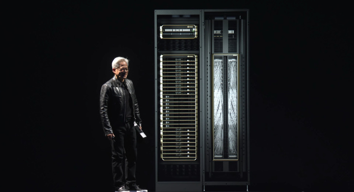
New high-performance systems like NVIDIA’s GB200 NVL72 or GB300 NVL72 use up to 8 power shelves per rack. These are large-scale AI compute systems designed for training and running massive AI models.
During the 2024 OCP Global Summit, NVIDIA announced that it has contributed the NVIDIA GB200 NVL72 rack and compute and switch tray liquid cooled designs to the Open Compute Project (OCP).
It is a rack-scale AI system that contains: 72 GPUs, 36 CPUs, high speed NVLink, switches and power units.
What is the Open Compute Project?
OCP was initiated by Facebook as an effort to build the most energy-efficient data center. In 2011, Facebook open-sourced the designs and formally launched the OCP.
Meta (then called Facebook), Intel, Rackspace, Goldman Sachs, and Andy Bechtolsheim are the founding members. Today it is a non-profit organization with the Board of Directors being represented by executives from Meta, Intel, Microsoft, Google, etc
At the core of the foundation, it is a place where creativity and ideas can be shared in order to create scalable computing hardware and servers that adapt to needs.
In 2011, Meta opened their first data center in Prineville, Oregon when they wer about to hit a billion Facebook users. It was 38% more energy efficient with state-of-the-art cooling system. This was the industry’s first data center that had a power usage effectivness (PUE) of 1.07. When they started designing the Prineville data center, the prevailing average of the industry was 1.9.
Later in 2013, they launched the Networking Project, which created a disaggregated network switch that made it easier to scale data center technologies and modify the software that runs on them.
In 2014, they announced Wedge, a top-of-rack switch, and FBOSS, a Linux operating system. These were used to develop Backpack and Minipack - modular platforms that enabled us to modify any part of a system without hardware and software interruptions.
In 2015, they released 6-pack, a modular platform that allows engineers to modify any part of a system without hardware and software interruptions.
In 2016, The OCP model and success inspires creation of TIP, an open approach to telecom network infrastructure.
HPE’s ProLiant servers use OCP 3.0 NIC. Most of AT&T’s network is running OCP switches. What it does is it allows room for a company to innovate and differentiate themselves, while ensuring that their product roadmap aligns with what the hyperscalers and the rest of the world is doing, and what the customer demands.
NVIDIA and Meta are both contributing modular server and rack technologies; the former its MGX based GB200-NVL72 rack and compute and switch tray designs; the latter introducing Catalina AI Rack architecture for AI clusters.
Why did we transition from 12V to 48V to 54V?
The shift is majorly due to improvement in efficiency caused by reduced resistive Losses (I^2R). Lower current significantly reduces resistive losses. And since we are continuosly trying to increase the power output, its optimal to increase the voltage. Ofcourse, there are a variety of challenges while scaling the voltage. Not all existing data center equipment and components are compatible with 48V or 54V DC input power. Electromagnetic interference (EMI) and electromagnetic compatibility (EMC) is a challenge since modern power electronic converters used in high-voltage DC systems, operate at higher frequencies.
As part of the Open Compute Project (OCP), Google pioneered the move from 12V to 48V DC around 2016 which helped scale rack level power from 10 kW to 100 kW. As AI compute power needs per rack reach 1 MW, there is a need to go to even higher DC rack voltages.
Google was a latecomer to the OCP. In 2009, Google started evaluating alternatives to their 12V power designs. The development of 48V rack power distribution was kicked off in 2010; it was at least 30% more energy efficient as it eliminated the multiple transformer stages.
The proposed Open Rack 2.0 standard specified a 48V power architecture with a modular, shallow-depth form factor that enables high-density deployment of OCP racks into data centers with limited space.

The shift to 54V came with Open Rack 3.0 (ORV3). A crucial aspect of this change relates to battery charging requirements. For instance, a fully charged 48V lead-acid battery system would typically float charge around 54.5 VDC, to ensure optimal battery performance and longevity. Moving to a 54V standard for the power shelves and infrastructure aligns it more closely with the actual voltage requirements of the battery backup systems.
Overall rack power could reach 13kW or more using this 48V. ORV3 power shelves are designed to accommodate higher power requirements, with options to support 33kW.
Why 54V Power systems are reaching their limits?
If scaled with 54V, racks would require so many power shelves that there would be no space left for compute hardware. One 1 MW rack could need 64U worth of power shelves - the height of an entire rack. A standard server rack is 42U to 60U tall, where 1U equals 1.75 inches. To fix this, NVIDIA showed a new solution at their GTC 2025 event: an 800V “sidecar” - a separate power unit that can power 576 GPUs in just one rack. Instead of converting power at each rack or server level, the sidecar performs one centralized AC-to-DC conversion at 800 volts. This high-voltage DC is then distributed to the GPUs.
As power usage from a single rack scales to 500 kW - 1 MW, using 54 V rails is simply not possible. This will require 200 kg of copper busbar for a single MW-rack. A GW-class datacenter would then consume half-a-million tons of copper which is half the copper mined in the US. The only alternative is go to higher voltages. The goal is to jump from 200kW per rack to 1MW and it has to be made feasible through a combination of transformative changes in power delivery, advanced liquid cooling technologies, and innovative rack designs.
At 54V, delivering 1 MW requires many power shelves, which take up rack space. At 800V, the same power can be delivered with fewer shelves, thinner cables, and less cooling infrastructure. This means more of the rack can be used for compute hardware (GPUs, CPUs), not power conversion. So for every Megawatt of power, you get more usable compute space with 800V than with 54V. The 800V architecture saves space per megawatt of power delivered.

Today’s racks rely on 54 V DC power distribution, where bulky copper busbars shuttle electricity from rack-mounted power shelves to compute trays. As racks exceed 200 kW, this approach begins to hit physical limits.
What is the proposed 800V architecture?
By converting 13.8 kV AC grid power directly to 800 V HVDC at the data center perimeter using industrial-grade rectifiers, most intermediate conversion steps are eliminated. This streamlined approach minimizes energy losses, which typically occur during multiple AC/DC and DC/DC transformations.
With a single-step AC/DC conversion, the system benefits from a more direct and efficient power flow, reducing electrical complexity and maintenance needs.
Using 800 V busways and switching from 415 V AC to 800 V DC in electrical distribution enables 85% more power to be transmitted through the same conductor size. This happens because higher voltage reduces current demand, lowering resistive losses and making power transfer more efficient.
 at the boundaries between power room and hall, hall and row, and at the row level to the IT racks.")

Up to 5% improvement in end-to-end power efficiency
Maintenance costs reduced by up to 70% due to fewer PSU failures and lower labor costs for component upkeep.
With lower current, thinner conductors can handle the same load, reducing copper requirements by 45%.
Lower cooling expenses from eliminating AC/DC PSUs inside IT racks
Which companies are enabling this change?
NVIDIA is collaborating with key industry partners across the data center electrical ecosystem, including:
Silicon providers: Infineon, MPS, Navitas, ROHM, STMicroelectronics, Texas Instruments
Power system components: Delta, Flex Power, Lead Wealth, LiteOn, Megmeet
Data center power systems: Eaton, Schneider Electric, Vertiv
Just as STMicroelectronics reaped the fruits of Tesla’s early push for SiC, Infineon and Navitas are jockeying to profit from the emerging GaN moment driven by Nvidia.
Infineon is a leading provider of power semiconductor solutions. Their expertise spans the entire power delivery chain.
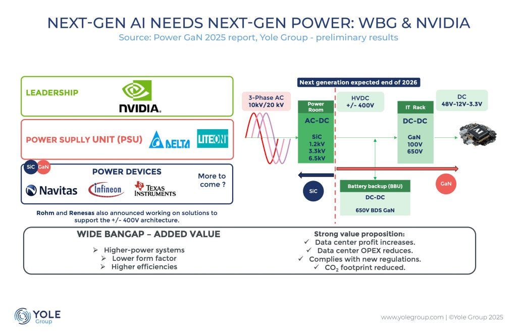
Traditional data centers convert 13.8 kV AC to lower AC voltages, then to a lower DC voltage at the IT rack, and finally to a lower AC voltage to power GPUs.
13.8 kV AC grid power is converted to 800-volt HVDC at the perimeter, and then from 800-volt HVDC to the lower voltages needed to run graphics processing units (GPUs) in the IT rack.
SiC chips are essential in converting grid power to 800-volt HVDC at the perimeter. Gallium nitride (GaN) chips are used to switch from 800-volt HVDC down to the lower voltages necessary at the IT rack because GaN can switch at a higher frequency allowing for smaller and more efficient power conversion.

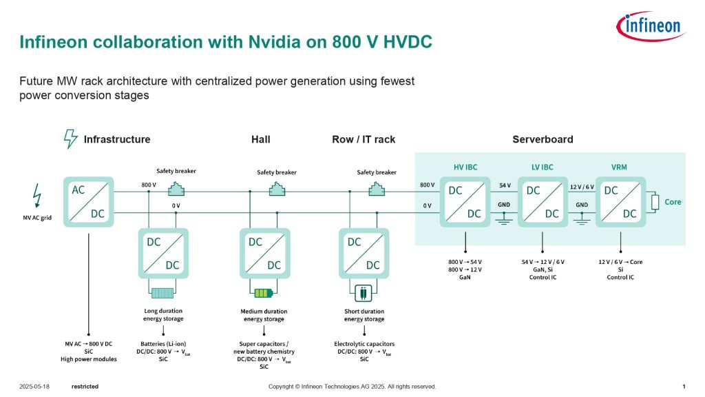
The left half shows the rack equipment, BBU is Battery Backup Unit, and Super-cap is Super Capacitor-based power supply equipment. The IT tray shows the inside of each server.
As we move towards the 250KW to 1MW era in the future, the method of power supply from the power grid will change significantly

If you only focus on “performance per watt” , you miss the bigger picture. It's not enough to make efficient chips because the scale of computing has exploded. Even though each chip is better, the total usage is continuously going up.
Year Processor Power (xPUs) Server Rack Power
2022 ~ 0.4 kW ~ 60 kW
2023 ~1 kW ~100 kW
2024 ~2 kW >150 kW
2027 2–4 kW 600 kW – 1 MW
Nvidia named Navitas as a technology partner for its wide band gap semiconductor technology. Navitas Semiconductor is the only pure-play industry leader in gallium nitride (GaN) power ICs and silicon carbide (SiC) technology. It also dabbles in 48 Volt down to power the processors.
Navitas has also developed a patented digital control technique called IntelliWeave that enables peak efficiencies of 99.3% for the power factor correction stage and reduces power losses by 30% compared with existing solutions.
Ultra-high-voltage SiC technology will be essential in developing “solid state transformers” connected to the grid. Beyond data centers, grids are getting upgraded to solid-state transformers everywhere.
What are wide-band gap semiconductors?
In 2018, Tesla inverted our expectations and shook the EV industry when they adopted an STMicroelectronics SiC based inverter for their new Model 3 electric vehicle. It allowed Tesla to shrink one of an EV's most critical components in half, and it has sparked new interest in a silicon technology as old as the industry itself. It has been a game changer for the power electronics industry.
Semiconductor materials have something called a valence band and a conduction band. When electrons get too much energy and get too excited they break into the conduction band. Now they are charge carriers. When electrons are in the conduction band, the transistors cannot switch meaning it is always conducting and cannot return to the off state.
The band gap represents the amount of energy needed to make electrons jump out of the valence band and into that conduction band. The wider the buffer zone, the more energy needed to jump the bands.
A number of materials including boron nitride, silicon dioxide and even diamond are all defined as WBG materials.
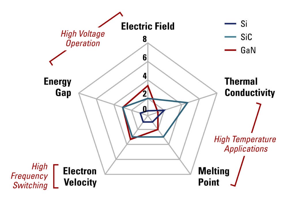
Why SiC over Si?
SiC not only has a super wide band gap but is also an excellent conductor of heat - 3 times better than traditional silicon and second only to diamond. It can go from 300 - 900°C with the right packaging.
As the voltage in a power device increases, their electric fields get stronger. When the field gets powerful enough, the device suffers what is called an avalanche effect - atoms break down and release large numbers of free charge carriers, leading to very large currents moving through materials.
SiC's critical electric field limit before this avalanche effect breaks out is 8 to 10 times higher than that of traditional silicon. It can handle voltages as many times higher than silicon.
Because of its wider band gap, SiC based power electronics can operate at -
Up to 10× higher temperatures
Up to 10× higher voltages
Up to 5× higher switching frequencies
Compared to silicon that has a band-gap of 1.12 eV (electron-volts), GaN and SiC are compound semiconductors with band-gaps that are around three times higher at 3.39 eV and 3.26 eV respectively.
The higher electron mobility of GaN, for example, makes it much more suitable for high-performance, high-frequency applications, something that is further supported thanks to a very, very small percentage of the chip being actually consumed by the gate electrode. This ensures very low capacitance meaning it is easy to achieve higher frequencies which is why GaN semiconductors are widely used in RF devices that switch in the gigahertz range.
SiC, on the other hand, with its higher thermal-conductivity and lower-frequency operation is more suited for higher-power applications including the higher-end voltages
Today, many of these power electronics are silicon-based.
The two most popular power switching devices are:
Insulated Gate Bipolar Transistor (IGBT)
Silicon-based IGBT devices are used for high voltage, high power, and low frequency applications. Most EV inverters before the Model 3 use IGBT transistors.
Power Metal Oxide Semiconductor Field Effect Transistor (MOSFET)
Silicon-based MOSFETs are for low voltage, lower power, and high frequency applications. They dominate the market for applications below 600 volts.
These circuits are placed near jet turbines or car engines in harsh environments with temperatures ranging up to 225°C or higher.
Silicon carbide (SiC) has become popular in the automotive industry and is also commonly used in solar panels and data centers. You can thank Gallium nitride (GaN) for the ability to charge your smart devices faster; from 2019 to 2024, GaN helped fast chargers increase from 50 to 240 watts.
Monolithic Power Systems, MPS with a market capitalization of 36 billion has solidified its place as a top tier supplier in the chip sector. While IDMs dominated by providing the assurance of long-term supply to industrial clients, the new market dynamics are shifting power towards fabless companies.
What are the challenges?
Producing enough high purity SiC wafers is hard. Today, Silicon wafers are made by first creating a big silicon crystal using the Czochralski method which involves growing a big crystal by repeatedly dipping a seed into the molten silicon melt. This method does not work for SiC because it sublimes before it melts. We need to grow our silicon carbide crystals from gas.
In 2001, Infineon introduced the first commercial SiC-based power device in the form of a Schottky diode. Later in 2010, Wolfspeed commercialized the first SiC MOSFET. Other companies like STMicroelectronics, ROHM, Infineon, Microsemi joined.
GaN cannot be grown on native substrates easily. High-quality GaN layers require precise epitaxial growth techniques like MOCVD (Metal-Organic Chemical Vapor Deposition). The deposited material grows in a specific crystal orientation, matching the underlying substrate. MOCVD tools are used in the production of GaN-based LEDs, which are widely used in lighting and display applications.
GaN was used in LEDs and RF devices in the 90s. Research into GaN for power electronics accelerated and commercializing started in the 2010s and now the adoption has entered automotive and industrial sectors.
Interesting tidbit
The most profitable component in Nvidia's AI server is the server rail kit - 76% gross margin for Kingslide vs 71% for Nvidia.Kingslide is a Taiwanese supplier that makes the custom rail kits used to rack and service heavy AI servers inside hyperscaler data centers.

References -
https://developer.nvidia.com/blog/nvidia-800-v-hvdc-architecture-will-power-the-next-generation-of-ai-factories/
https://www.yolegroup.com/strategy-insights/nvidia-defines-power-electronics-future/
https://www.infineon.com/press-release/2025/INFXX202505-107
https://www.powerelectronicsnews.com/powering-the-future-how-nvidia-and-infineon-are-reinventing-ai-data-center-architecture/
https://news.mynavi.jp/techplus/article/20250714-3377236/
https://navitassemi.com/introduction-to-wide-bandgap-semiconductors/
https://tech.facebook.com/engineering/2021/11/open-compute-project/?ref=thestack.technology